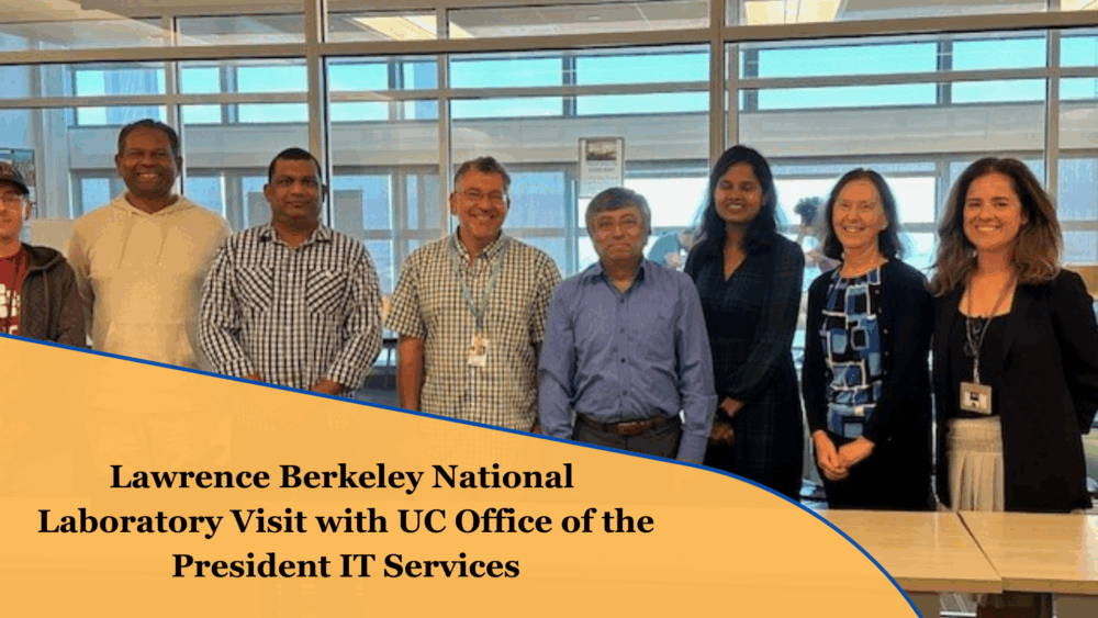
When I saw the opportunity to tour Lawrence Berkeley National Laboratory (Berkeley Lab), I didn’t think twice. The Berkeley name alone convinced me—and it was also a chance to meet my colleagues from the Information Technology Services (ITS) Engagement Committee at the UC Office of the President (UCOP).
From the start, the event was exceptionally well organized. Melissa Katzin, System Support Analyst, and Laurel Skurko, Marketing Professional, from the UCOP ITS Engagement Committee, did a fantastic job coordinating everything. Evren Essner, Head of Protocol from Berkeley Lab, was equally helpful, sharing all the necessary information and maps ahead of time.
Since it was my first visit to Berkeley Lab, I took BART and then the Berkeley shuttle. I almost got lost, but luckily, I bumped into my ITS Engagement Committee teammates. We were warmly welcomed by Evren and spent a few minutes in the waiting room while Shirley Bittlingmeier, Client Services Officer, and Sushant Prasad, Solutions Architect for AWS Cloud, shared their fond memories of studying at UC Berkeley.
Meeting Adam Stone, CIO
Our tour began with Adam Stone, Chief Information Officer (CIO), in the conference room. He gave us a fascinating overview of LBNL, which was founded by Ernest Orlando Lawrence, the inventor of the cyclotron, a type of particle accelerator developed at the University of California, Berkeley, Lawrence Berkeley National Laboratory.
Adam highlighted LBNL’s key national user facilities, including:
- Advanced Light Source (ALS): The “beating heart of the laboratory,” a synchrotron light source generating X-ray, infrared, and extreme ultraviolet light, supporting the research of thousands of users annually.
- Joint Genome Institute (JGI): Supports the Department of Energy’s (DOE’s) clean energy and environmental research.
- Molecular Foundry: DOE-funded nanoscience research facility.
- ESnet: The Energy Sciences Network, DOE’s dedicated science network.
- National Energy Research Scientific Computing Center (NERSC): Supports DOE-funded projects requiring high-performance computing (HPC).
Adam also shared his personal journey, the challenges he faces in his role and some exciting ongoing projects, including a genome-based large language model (LLM).
Tour with Bill Arndt
Next, Bill Arndt, Computer System Engineer, who holds a PhD in Computer Science, guided us through the tour. Bill provided clear instructions before the tour, emphasizing safety and engagement. We explored the Perlmutter system, National Energy Research Scientific Computing Center (NERSC)’s flagship system, housed in the center’s facility in Shyh Wang Hall at Berkeley Lab and installed in 2021. It is scheduled to be decommissioned next year, to be replaced by Doudna, built on Dell Integrated Rack Scalable Systems and NVIDIA CPU-GPU platforms.
Key highlights of the tour included:
- Learning how the facility in Shyh Wang Hall is seismically engineered.
- Seeing the high-efficiency cooling system in action.
- Observing the robots that move storage drives in and out of racks.
- Opening a rack and even touching a supercomputer, which was a thrilling experience.
Bill also showed us the preparation underway for the new supercomputer and explained the significant costs and planning involved in adapting a space to accommodate such a system. All our questions were answered, leaving us feeling privileged and inspired by the experience.
Our tour Lisaison, Evren walked us out of the building, and as we left, I realized it had truly been a special day—full of learning, inspiration and connection with colleagues.
You can’t imagine how proud I felt just standing next to the photo of LBNL scientists who are Nobel Prize recipients—and how incredible it was to touch the supercomputer.
So, next time an opportunity like this comes along, take it—it’s truly worth it. And who knows, maybe the Advanced Light Source (ALS) will be my next stop!
Thank you to all attendees/participants:
- Lawrence Berkeley National Laboratory (LBNL)
- Adam Stone — Chief Information Officer (CIO) & IT Division Director
- Evren Essner — Head of Protocol, Laboratory Directorate
- Bill Arndt — Computer System Engineer
- UC Office of the President (UCOP)
- Beena Albert — Business Intelligence Technical Lead, ITS
- Samson Bali — Technical Support Analyst, IT Client Services
- Shirley Bittlingmeier — Executive Director, IT Client Services (ITS)
- Jackie Porter — Cyber Risk Technical Project Management Coordinator
- Melissa Katzin — System Support Analyst
- Sushant Prasad — Solutions Architect, AWS Cloud
- Sundar Potti — Business Systems Analyst
- Laurel Skurko — Marketing
Resources
- RESOURCE: Lawrence Berkeley Laboratory (website)
- RESOURCE: Take a Virtual Aerial Video Lab Tour (2 minutes) (or sign up for a public or private tour)
- RESOURCE: Request a Private Tour: Berkeley Lab
- RESOURCE: Doudna / National Energy Research Scientific Computing Center (NERSC) (website)
- May 29, 2025, DOE Announces New Supercomputer Powered by Dell and NVIDIA to Speed Scientific Discovery, Berkeley Lab News
Author
Beena Albert
Business Intelligence Technical Lead, ITS
UC Office of the President
[Cover photo caption/alt text: Pictured, from left to right: Bill Arndt, Samson Bali, Sundar Potti, Adam Stone, Sushant Prasad, Beena Albert, Shirley Bittlingmeier and Evren Essner]